Abstract
The propose exhibits a tunable low noise amplifier (LNA), which provides the tunability at sub-GHz frequency range and hence can become choicest frequency range for 5 G applications. Common source (CS) with source degeneration inductor LNA is proposed; in which the inductor in source branch is replaced by gyrator-c active inductor which not only reduced the overall area of the circuit but can also be used to provide the feature of tunability by changing the bias voltage of CMOS based active resistor in feedback branch. Therefore, instead of having a LNA circuit for the fixed frequency, a single tunable LNA design can be used over a range of frequency from 1 GHz to 5 GHz. The proposed approach will provide the direct tuning to the circuit. The forward voltage gain achieved is greater than 10 dB, input matching parameter is less than −10 dB and the output matching parameter is less than −10 dB. The average power dissipated is 0.02 W. The results can be tuned by controlling the feedback voltage of tunable active inductor (Tunable_AI). The tunable results can be achieved up to the bandwidth of 1 GHz.
1. Introduction
The availability of wireless communications has facilitated the connection of a vast number of individuals to the internet, enabling them to leverage the advantages of the contemporary digital economy. Wireless technologies have become essential in today's economy, serving critical functions in sectors ranging from banking and agriculture to transportation and healthcare. Furthermore, emerging technologies like 5 G services, AI based systems, and the Internet of Things (IoT) depend heavily on robust wireless communication networks and have the potential to transform our lives at an unprecedented scale and pace. With the increased mobility and collaboration helps the users to stay connected easily and the programmability is increased to have a good expandability. The ever-demanding interest to have wireless communication and to have a complete system on a single chip lead to the motivation to increase the performance parameters of each block of any radio frequency integrated circuits (RFIC).
The low noise amplifier (LNA) is an elementary part in the transceiver cell and has a significant effect on the functionality of the radio receiver. As a main block in the wireless section, it should give low Noise figure (NF), good reflection coefficient (S11), bandwidth, linearity, and dynamic range. It should also provide good gain. One of the methods to provide tunablity is by using a MOS varactor in accumulation mode as shown in [1]. In this work, the inductively degenerated CS LNA has been redesign for the application of sub-GHz frequency range i.e., up to 5 GHz. The range of frequency used for the design is also applicable for WSN applications [2, 3]. Content includes the device level variables. This paper is categorized into three parts. Section 2 gives the brief introduction about LNA topologies. Section 3 will give us the idea about the practical design considerations. Section 4 explains the proposed design of tunable LNA. Model outcomes of tunable LNA are explained in section 5 and lastly the paper is wrapped up in section 6.
2. Fundamentals of LNA and topologies
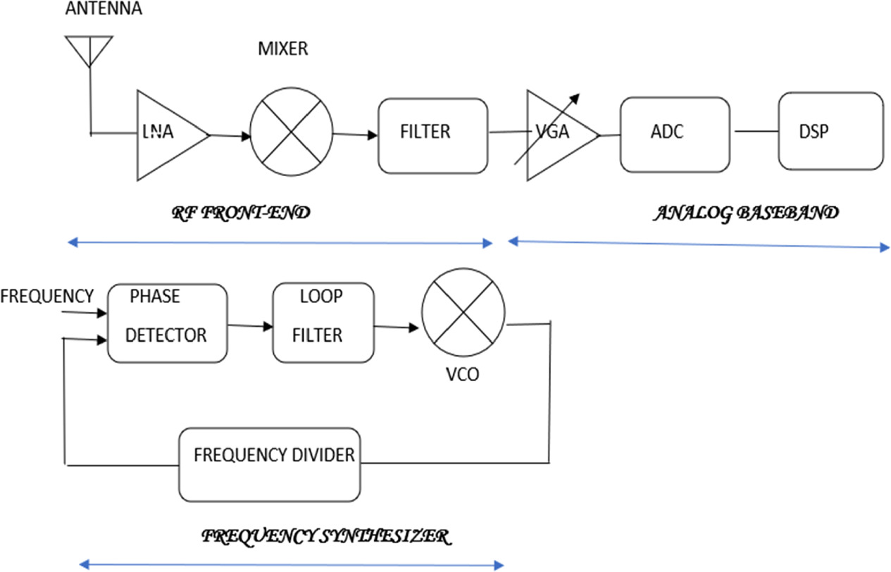
The Low-Noise Amplifier (LNA) serves as the initial component in a communication system's receiver section and is directly linked to the RF antenna, as seen in figure 1 [4]. The performance of the receiver is significantly impacted by the noise figure (NF) and scattering parameters of the LNA.
Figure 1. Basic Block Diagram of RF- receiver.
Download figure:
Standard image High-resolution imageThere are four distinct topologies available for designing an LNA circuit, each with its own advantages and disadvantages. Based on the user's needs and the specific application, a single approach, or a cascaded combination of them may be employed. These topologies are (a) CS with shunt resistor topology (b) Shunt series feedback common source (c) CS with Inductor Degeneration (d) Cascode with Inductor Degeneration. The most utilized methods for CMOS LNA design are CS common source design and CG common gate design. Among these, the common source LNA offers reasonably higher gain and superior results compared to other methods. Conversely, the common gate designs yield a low-power, less parasitic and more stable circuit at the expense of noise performance. To enhance noise performance in the CG configuration, capacitive cross-coupling methods may be employed. These two techniques are the preferred options for broadband LNA circuits [5]. The shunt or parallel feedback LNA is commonly utilized when a wide frequency range input-output match is necessary. This approach typically yields moderately high linearity. The addition of inductors to the circuit can enhance the performance of high-frequency circuits. A design technique that employs an inductor in the source branch has the benefit of aiding designers in achieving excellent input matching. Inductive components at the source terminal of the MOS can replace the reactance at the input stage [6]. LNAs are designed to decrease the undesired signal generated by the amplifier. However, the presence of rain causes attenuation in the propagating electromagnetic waves, leading to the reception of distorted signals by the antenna. To address this, a low noise amplifier (LNA) has been devised and proposed in [7] which indicated to enhance the received signal strength—both in terms of gain and reduction in noise figure. This improvement enables more accurate detection of radio signals reflected from the Earth surface at the receiver of aircraft. The LNA design incorporates inductive source degeneration, a stability-enhancing technique that has proven to be both feasible and optimal. On the other hand, the cascode method is used where the large bandwidth is required. In this work the common source with degenerated inductor has been used and the novelty of the work is that the passive inductor in the source branch is replaced by gyrator-C based active inductor which is tuned by using active resistor and is named as tunable_active inductor (Tunable_AI) as it will consume the lesser area and the tuning of the inductor is done by direct method by controlling the bias voltage of the feedback element.
3. Practical considerations of LNA
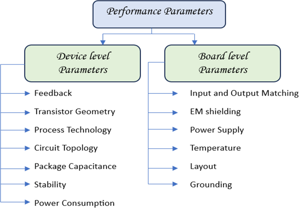
The performance of LNA depends on various set of parameters that can be classified into device level and board level. Figure 2 shows the parameters which can be kept in mind while designing an LNA. In this work the stability of the design is checked by achieving a stable gain and s-parameters over the required frequency range. The device performance is also dependent on the transistor dimensions and the package type as shown in figure 2 [8]. So, these should also be considered while design implementation. Process technology and circuit topology are the parameters that affects the circuit performance at device level whereas, I/O matching, layout and EM shielding affects at board level [9, 10] as depicted below.
Figure 2. Performance parameters for LNA.
Download figure:
Standard image High-resolution imageIn this work, we focus to enhance the characteristics of LNA at device level for the sub-GHz frequency range. The target frequency of the design is up to 5 GHz which is the choicest frequency range for 5 G wireless communication. The main offering of the paper is to provide the direct tunability in the circuit which is done by variation in the bias voltage applied to the gyrator -C active inductor of source degenerated LNA circuit. By selecting the relevant active inductor, the overall performance of the device can be enhanced. At very high frequencies, there are two main challenges. The first one is parasitic, which can cause stability issues and decrease output-to-input isolation.
The second challenge is related to the limited voltage supply when circuits need to operate from a low voltage source. This limitation affects the circuit topology and transistor bias. One solution to this problem is to use a magnetic feedback Low Noise Amplifier (LNA), which is a simple structure consisting of an active device. The magnetic feedback topology is particularly well-suited for high-frequency applications, where parasitic capacitances can dominate and reduce reverse isolation, secondly a band-switchable low noise amplifier (LNA) is designed using a 0.13 μm SiGe BiCMOS process, allowing for operation at both 28 and 60 GHz frequencies. Furthermore, a tunable stub is employed at the output to enable seamless switching between the two frequency bands. The tunability of the stub is achieved through the utilization of an HBT switch [11]. In addition to magnetic feedback, various other techniques are used to analyze noise in circuits, the techniques include classical noise matching, simultaneous noise and input matching (SNIM), noise optimization under power constraints, and simultaneous noise and input matching under power constraints (PCSNIM) [12]. Transistor optimization can be done so that flicker noise at the front end of the analog circuits can be reduced [13]. A Cascoded LNA is presented which can be used for the application in 5 G circuits in the frequency range of 50–60 GHz [14]. Continuously stepped variable gain low-noise amplifier (CSVG-LNA) tailored for millimeter-wave (mm-wave) 5 G communications is used which realizes variable gain within a two-stage LNA structure through the integration of a tunable transformer in the second stage. The adjustable coupling coefficient of this transformer facilitates seamless modification of the LNA's output matching, enabling the realization of a CSVG-LNA design. By doing so, the proposed CSVG-LNA addresses challenges associated with excessive power consumption and significant fluctuations in noise figure (NF) that are prevalent in conventional methodologies [15, 16]. CS-LNA with degenerated inductor is given in [4], in contrast to that the inductor in source branch is replaced by a gyrator -C active inductor, to provide the tunablity in the circuit. The device uses an active phase shifter in the amplifier's feedback loop to change the phase of signal amplified as indicated in [17, 18]. Cascode structures [19, 20] can also be used to incorporate the advantages such as reduced Miller effect, large bandwidth and also noise figure can also be reduced. The reduction in power consumption using current-reused CG stage is shown in [21]. The frequency ranges from 1 GHz −5 GHz can also be used for the blue-tooth applications and the results are given in [22]. The RF CMOS CG based LNA design and CS inductively degenerated LNA design for the space exploration to achieve minimum power and good value of gain is depicted in [23].
4. Proposed design of LNA
The Target Design Specifications selected for the proposed tunable Low Noise Amplifier (LNA) is listed in table 1.
Table 1. Target design specifications of tunable LNA.
| Parameter | Freq range | Voltage gain | Input matching S11 | Output matching S22 | NF |
|---|---|---|---|---|---|
| Value | Up-to 5 GHz | 10 dB(min) | <−10 dB | <−10 dB | 3 dB max |
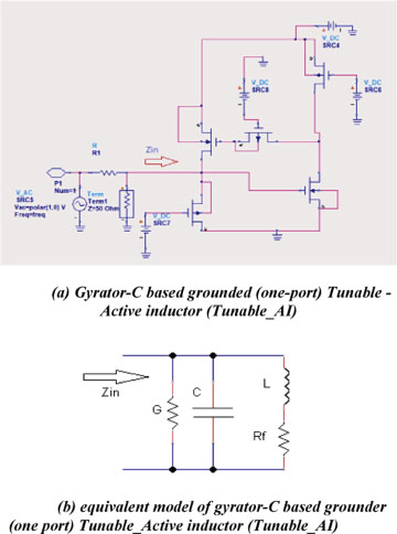
Aim is to design a LNA which can be tuned directly and can give the stable results. The proposed design can be tuned within 1 GHz bandwidth, and the overall chip area can be reduced by replacing the source degenerated inductor by gyrator-C tunable_active inductor (Tunable_AI). The design for Tunable_AI is shown in figure 3, which uses the active resistor in the feedback path and and the variation in inductance value can be achieved by changing the bias voltage SRC8 across the active resistor as shown in figure 5.
Figure 3. (a) Gyrator-C based grounded (one-port) Tunable - Active inductor (Tunable_AI). (b) equivalent model of gyrator-C based grounder (one port) Tunable_Active inductor (Tunable_AI).
Download figure:
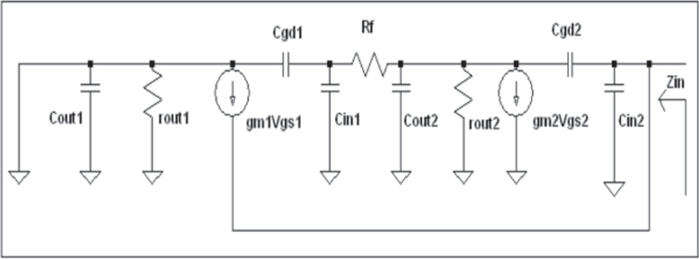
Standard image High-resolution imageThe design was analysed at GHz frequency range using the small signal equivalent model of the MOSFET, resulting in a complete high-frequency model of the circuit is shown in figure 4.
Figure 4. The small signal equivalent circuit of gyrator-type Tunable_AI at high frequencies.
Download figure:
Standard image High-resolution imageTo simplify the analysis, the 'bulk' and 'source' components are connected, and both transistors are assumed to be identical. As a result, the small signal model parameters for both metal-oxide-semiconductor field-effect transistors (MOSFETs) are identical, including the gate-to-drain capacitances (Cgd), and transconductances (gm1, gm2). The MOSFETs are biased using ideal current sources, and the gate-drain capacitances for both MOSFETs are neglected, resulting in a conductance equations (1) and (2).


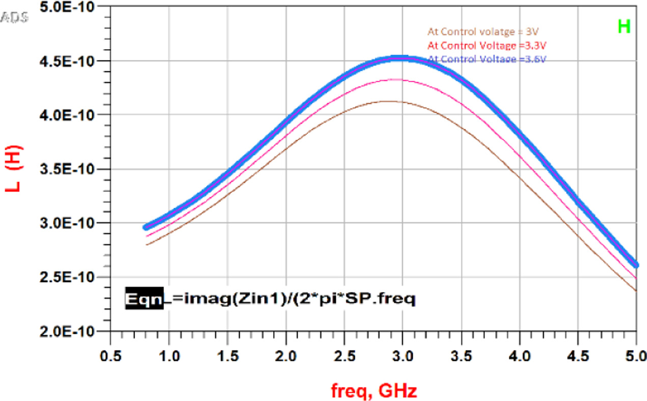
The simulation results by controlling the V_DC of SRC8 to have the variations in inductance value as shown in figure 5. The tunable ability is further used in LNA design, and the circuit can be tuned within 1 GHz bandwidth.
Figure 5. Variation in inductance with the variation in control voltage at SRC8.
Download figure:
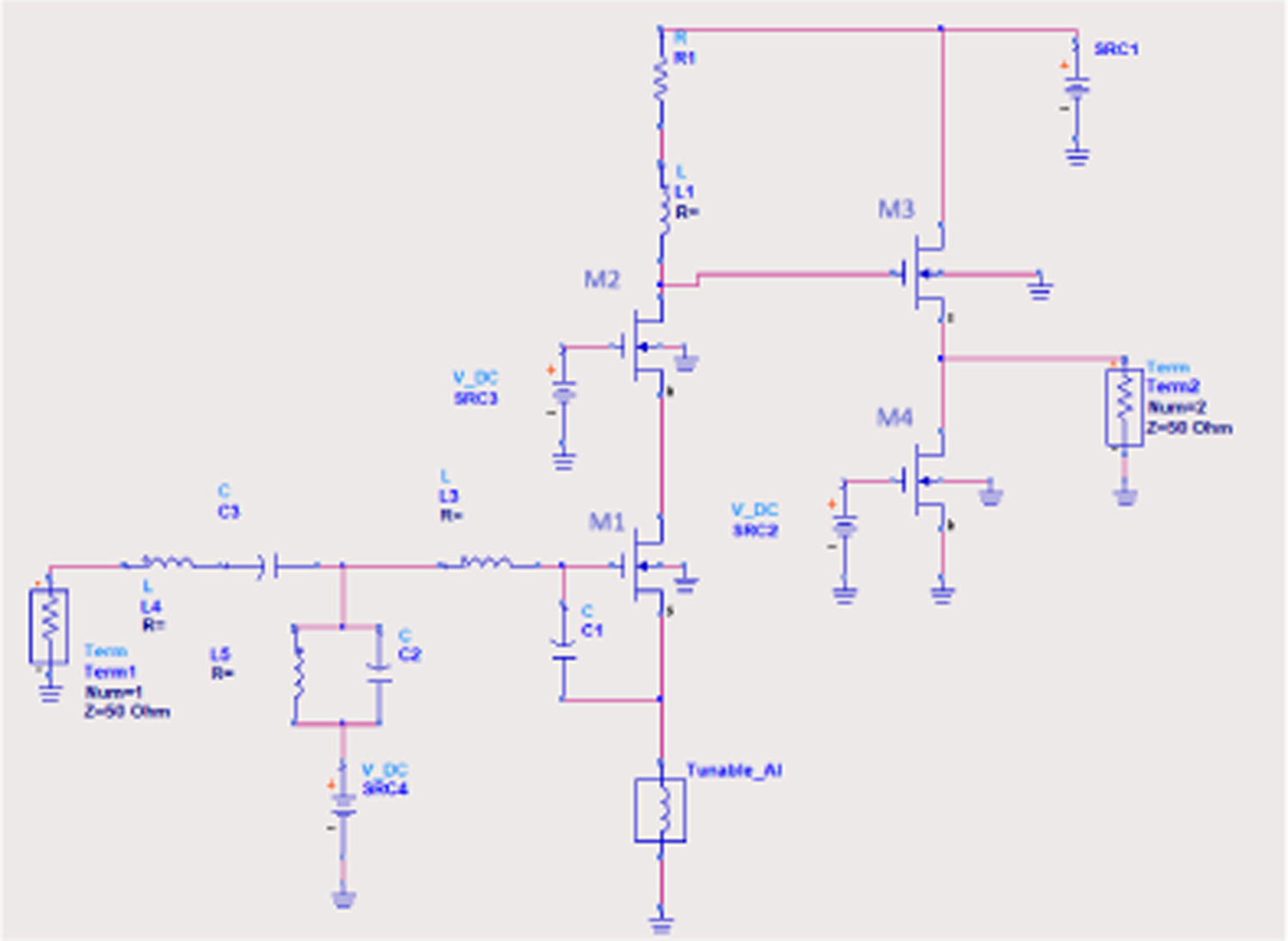
Standard image High-resolution imageThis active inductor design is utilized in CS-source degenerated LNA design. In designing a Low Noise Amplifier (LNA), it is important to simplify the circuit as much as possible to avoid introducing parasitic effects. The Low Noise Amplifier (LNA) design which is taken under consideration is the common source (CS) with source degeneration circuit as depicted in figure 6 because it provides the good matching in the narrowband frequency range. The source degeneration inductor is replaced by the gyrator-C based tunable_active inductor (Tunable_AI). The structure of tunable_AI consist of four MOS devices and the feedback resistance is replaced by active resistor in which bias volage can be varied to vary the inductance of the inductor as shown in figure 3(a). The circuit is simulated at 90 nm technology. The overall proposed design of tunable LNA is shown in figure 6. This LNA design approach utilizes the common source with inductive degeneration topology to achieve high linearity. The LNA operates at a power supply of 1.5 V and is matched to a 50 Ω input and output port using a matching network consisting of C1, C2, and a small inductor. According to the thumb rule, the value of transconductance (gm) should be 10times the value of bias current ( ) if (
 ) = 1 mA. For this circuit, the value of
  is 10 mA. If the device works in the weak inversion region, it is quite challenging to maintain linearity, and the device should operate in the saturation region. To achieve the best linearity, the overdrive voltage
  should be maintained at specific value if the device is operated at a certain current of any value. This means that the device is operating in strong inversion, and if
  goes below that specific value, gm increases for the same (
 ). The relation between
  and W/L is given by the formula defined below, and the total capacitance offered by the gate and drain terminal is given as equation (3).

And the gain of the circuit is given by equation (4)

Figure 6. Common Source (CS) LNA with source degeneration with Tunable_active inductor.
Download figure:
Standard image High-resolution imageFigure 6 shows the basic structure of a cascaded input transistor comprising an input transistor (M1) and a cascade transistor (M2) for isolation. The addition of a cascade transistor helps to reduce the drain-gate capacitance of the input transistor, which acts as a Miller capacitance. In addition, there are three inductors in the circuit: A single inductor, labelled as Tunable_AI that is tunable_active inductor, serves a dual role, operating as both an on-chip ground line and an off-chip ground plate. This inductor utilizes an active resistor as a feedback component for tuning across different frequency ranges. In contrast to existing methods outlined in table 2, which primarily employ either the MOS varactor method or off-chip tuning of passive inductors for frequency adjustment, our proposed approach introduces tuning via a CMOS-based active resistor. This work enables direct tuning within RF circuits. The other two inductors are used to tune the frequency of the Low Noise Amplifier (LNA).
Table 2. Summary of performance and contrast with published research.
| References | [9] | [11] | [12] | [13] | [4] | Proposed work |
|---|---|---|---|---|---|---|
| Technique | CS-Source Degeneration with MOS Varactor | DC Bias circuit of CS LNA | Cascoded CMOS LNA | CS-LNA with Degenerated Inductor | Impedance Transformers at input stage | Tunable LNA using Gyrator-C LNA |
| Technology | 180 nm | 90 nm | 90 nm | 90 nm | MIC | 90 nm |
| Freq (GHz) | 2 GHz-3 GHz | 2 GHz | 56 GHz | 2.4 GHz | 2.2–2.8 GHz | Up to 5 GHz |
| No. of Stages | 1 | 1 | 2 | 1 | 1 | 1 |
| Gain (dB) | 12–15 | 14.02 | 30.7 | 11 | — | Min 10 |
| NF (dB) | 2.2–2.9 | 0.825 | 3.92 | 0.58 | 1.4–4.8 | 3 dB max |
| Supply | 1.8 | 2.6 | 1.5 | 1.5 | 1.8 | 1.8 |
| S11(dB) | < − 12 | −11.22 | − 15.3 | −9.6 | −29 | < −10 |
| S22(dB) | < −22 | −17.76 | −23.1 | −22 | — | < −10 |
| S21 (dB) | — | — | 28.85 | — | 7–18 | 20 |
| S12 (dB) | — | — | −32.66 | — | — | −38 |
| Tuning Technique | Tuning of MOS varactor in accumulation mode. | Off-chip Tuning of passive inductor | Off-chip Tuning of passive inductor | Off-chip Tuning of passive inductor | On-chip tuning of inductor in tuning circuit | On-chip tuning of CMOS based active resistor. |
The parasitic gate-source capacitance of transistor M1 is represented by Cgs. To ensure proper matching, the source impedance should be matched to the input impedance of the circuit design. The CB or CG configuration of the second stage ensures isolation between the input and output. In a cascade amplifier, the input stage amplifies the current, while the voltage is amplified in the cascade stage. This results in magnification of both the voltage and power of the signal, making it suitable for both digital and RF circuit designers. Capacitors C2, C3 and inductors L4, L5 are used to form a filter and the values are selected precisely to have a resonance frequency. The values of various components are L1 = 600 nF, L2 = is replaced by tunable_active inductor (tunable_AI) design, L3 = 1.8 nH, L4 = 0.67 nH, L5 = 4.86 nH, C1 = 15.49 fF, C2 = 201.8 fF, C3 = 84.75 fF.
5. Simulation results of tunable LNA
One of the important steps before starting the analyses is to select the transistor which should provide high gain at low noise figure with the minimum possible current consumption at the frequency of interest. The transistor selected for the design is BISM4 and the simulation is done at 90 nm technology. The frequency range selected for the simulation is from 800 MHz to 4 GHz. The simulated result is compared with the previous simulated results and is tabulated in table 2.
This model is preferred due to its accurate representation of the intrinsic input resistance for RF, high-frequency analog, and high-speed digital applications. Additionally, it offers an accurate model for gate direct tunneling of multiple layer gate dielectrics. An S-parameter analyses is done with ADS design tool. S-parameters (or scattering parameters) are a common way to describe the behaviour of linear RF devices, such as amplifiers, over a wide range of frequencies. In the case of a Low Noise Amplifier (LNA), S-parameters are used to describe the input-output behaviour of the amplifier as a function of frequency.
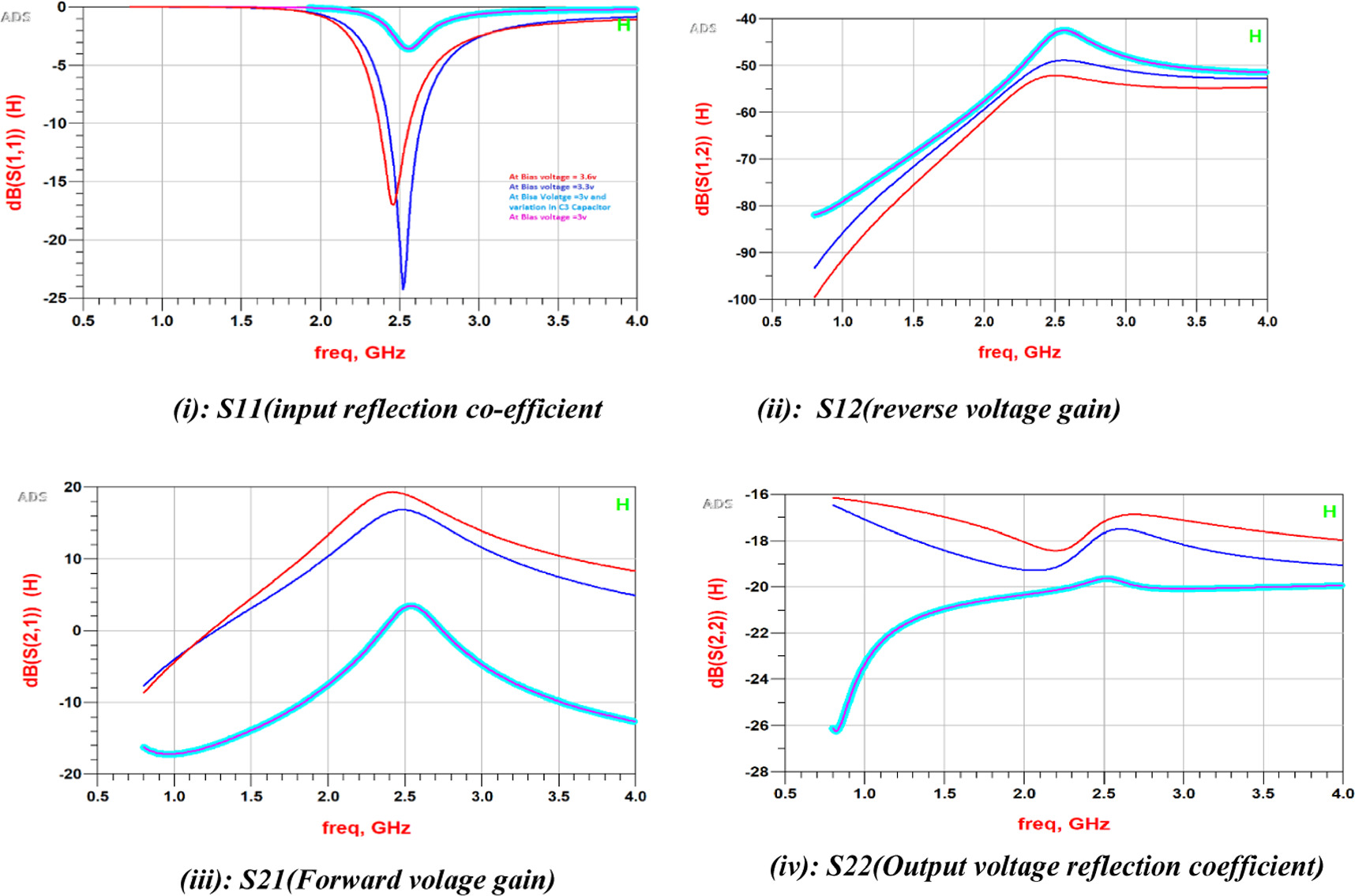
The S-parameters of an LNA consist of four values: S11, S12, S21, and S22. These values represent the complex ratios of the incident and reflected waves at the input and output ports of the amplifier. Four S-parameters that is S11(input reflection coefficient), S12(reverse voltage gain), S21(Forward volage gain) and S22(Output voltage reflection coefficient) are studies and the various results at different bias voltage is shown below from figures 7(i) to (iv).
Figure 7. (i): S11(input reflection co-efficient. (ii): S12(reverse voltage gain). (iii): S21(Forward volage gain). (iv): S22(Output voltage reflection coefficient).
Download figure:
Standard image High-resolution imageThe direct tuning is achieved by varying the capacitors C2 and C3 and by varying the internal bias voltage of tunable_active inductor (tunable_AI) the voltage gain can be increased or decreased. So, instead of using a fixed feedback resistor in gyrator-C active inductor, the feature of tuning can be introduced by using a MOSFET in a feedback path and by controlling the gate volage, the gain and other parameters of the Low Noise Amplifier (LNA) can be controlled.
S11, also known as the 'input reflection coefficient,' is a measure of how well an amplifier's input terminal matches the impedance of the source it is connected to. In a low noise amplifier (LNA), which is used to amplify weak signals, minimizing S11 is important for two reasons:
- 1.Maximizing power transfer: If S11 is high, a significant amount of the signal power may be reflected to the source instead of being delivered to the LNA. This can result in a reduction in the signal-to-noise ratio (SNR) of the system.
- 2.Reducing noise figure: The reflection coefficient (S11), which measures the noise contribution added to the signal by the amplifier, can have an effect on the noise figure (NF) of a low noise amplifier (LNA). Elevated S11 levels may result in more noise being reflected back to the source, raising the overall system's NF. Figure 7(i)'s graphs show that S11 values less than −10 dB are advantageous for 5 G LNAs. As a result, the NF is reduced because at least 90% of the input power is effectively directed into the LNA, with only 10% or less reflecting back to the source.
One of the most important factors in determining how well a Low Noise Amplifier (LNA) performs is the reverse voltage gain (S12). When the input signal is delivered to the amplifier's output and the output is terminated by a resistive load, it reflects the relationship between output voltage and input voltage. To get the best system performance, reverse voltage gain must be adjusted with other elements such as noise figure, stability, and power consumption.
In the context of 5 G applications, a desirable characteristic for a typical Low Noise Amplifier (LNA) is an S21 value of approximately 10 dB or higher. This indicates that the amplifier provides a power gain of at least 10 dB, effectively boosting weak signals within 5 G systems. S22, referred to as the 'output reflection coefficient,' gauges the degree to which an amplifier's output aligns with the impedance of the connected load. Within an LNA, an apparatus designed to amplify feeble signals, minimizing S22 holds significance for two key reasons.
- 1.Maximizing power transfer: If S22 is high, a significant amount of the amplified signal power may be reflected to the LNA instead of being delivered to the load. This can result in a reduction in the signal-to-noise ratio (SNR) of the system.
- 2.Reducing noise figure: S22 can also affect the noise figure (NF) of the LNA. A high S22 can cause additional noise to be reflected to the amplifier, increasing the NF of the system.
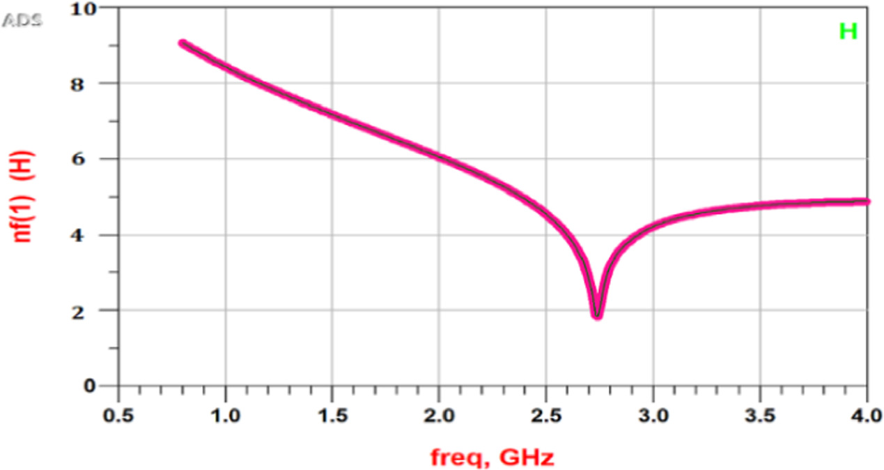
For a typical LNA used in 5 G applications, an S22 value of less than −10 dB is considered good. As depicted in figure 7(iv) the values are in the acceptable range and at least 90% of the output power is being delivered to the load, and only 10% or less is being reflected to the amplifier. The noise figure as shown in figure 8 is a crucial measure of a low noise amplifier's (LNA) ability to amplify signals without adding extra noise. It's calculated as the ratio of the total noise power output (including the noise generated internally by the LNA) to the noise power at the LNA's input. A low noise figure implies a higher signal-to-noise ratio and improved sensitivity.
Figure 8. (v):NF (Noise figure).
Download figure:
Standard image High-resolution imageTo achieve the better noise figure in the required frequency range, the LNA should also be designed with a suitable bias point to ensure that the transistor is operating in its most linear and low noise regime. And the average power dissipated by the circuit is 0.02watts at 90 nm technology.
6. Conclusion
The study explores the tunability of a Low Noise Amplifier (LNA). Using the ADS design tool, the LNA circuit is meticulously crafted and simulated, utilizing BSIM4 transistors at a 90 nm technology node. The circuit is optimized to operate within a bandwidth range of 1 GHz, with an emphasis on minimizing its overall footprint through the integration of an active inductor. Achieving a forward voltage gain of over 10 dB, coupled with input and output matching parameters below −10 dB, highlights its efficacy. Tuning the results is facilitated by regulating the feedback voltage of the tunable active inductor, which relies on a CMOS-based active resistor, thus enabling direct tuning. This tuning capability extends to the 1 GHz bandwidth. In the realm of Low Noise Amplifier (LNA) design, the ability to fine-tune gain and operating frequency post-manufacture holds great promise for the advancement of Radio Frequency Integrated Circuit (RFIC) technology. Such adaptability makes RFICs suitable for various applications, including Bluetooth and Wi-Fi hardware. However, a notable limitation of the design is its reliance on the direct tuning method to adjust gain and other parameters across the desired frequency spectrum.
Data availability statement
The W/L values and the values of passive components will be provided on reasonable request. The data that support the findings of this study are available upon reasonable request from the authors.
