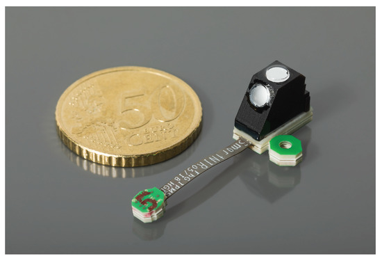
<p>Smart NIR spectrometer, optical bench measuring 6.5 × 10 × 10 mm<sup>3</sup> on a printed board with mounting bail and flat wire to connector; 50 Euro cent coin for size indication.</p> Full article ">Figure 2
<p>In the ongoing process of digitalization, networking is emerging at machine and factory level. Local data processing enables high availability with low latencies. In this architecture, programmable logic controller (PLC) for controlling actuators can directly access processed sensor data.</p> Full article ">Figure 3
<p><span class="html-italic">AnniNet</span> is essentially made up of three components. An encoder network, which extracts the features through a convolutional layer and then condenses them. A decoder network, which is used in training to improve feature extraction. And the evaluation of the spectral information is done in a regression network of dense layers, here the non-linear and overlapping spectral features can be evaluated. In addition, prior knowledge, for example the sample temperature, can be added to the regression network.</p> Full article ">Figure 4
<p>Grape harvester during harvest in the vineyard.</p> Full article ">Figure 5
<p>Shown is the first derivative of the measured absorbance of all samples at a sample temperature of 20 °C. For a better representation, a SNV was carried out. The confidence interval shows the differences between samples with different sugar and acid contents.</p> Full article ">Figure 6
<p>The attribution maps show the regression error caused by mask-ing out individual spectral bands. Areas marked in red have a high importance for the regression of the corresponding target parameter.</p> Full article ">Figure A1
<p>MEMS chips with tiltable grating, integrated position sensor and two slits in one device; left image shows the front side, right image shows the rear side with the cavities etched into the chip.</p> Full article ">Figure A2
<p>Stacked component spectrometer (“Sugar cube spectrometer”), left in the image the optical bench is depicted, fiber to a standard SMA head which indicates size on the right side of the image.</p> Full article ">Figure A3
<p>Principle of a scanning mirror micro spectrometer: 1: entrance slit, 2: collimation mirror, 3: mirror plate, 4: fixed grating, 5: refocusing mirror, 6: exit slit, 7: detector element.</p> Full article ">Figure A4
<p>Folded optical bench for a MEMS based micro spectrometer, the fixed grating is in the left middle, both off-axis mirrors were realized in one substrate placed in the upper region of the substrate, printed board with scanner mirror and detector unit is not shown here.</p> Full article ">
